WAFER FAB
Wafer Fab represents clean rooms and lines for IC pattern and discrete device generation on semiconductor wafers
The total production capacities of the wafer fab, classes 1, 10, 100, 1000:
200 mm silicon wafer processing, 0.35 µm technology - 8.4 k pcs/year
150 mm silicon wafer processing, 0.8 µm technology - 78.5 k pcs/year
100 mm silicon wafer processing, 1.2 µm technology - 355 k pcs/year
100 mm silicon wafer processing, 2.0 µm technology - 180 k pcs/year
WAFER FAB
100, 150, 200 mm monocrystalline silicon wafers for manufacture of microelectronic devices:
- 100 mm wafers for microelectronic devices, >1.2 µm technology;
- 150 mm wafers for microelectronic devices, 0.8 µm technology;
- 200 mm wafers for microelectronic devices, 0.5 - 0.35 µm technology.
Capacities
Manufacture of monocrystalline silicon wafers for microelectronic devices:
- 100 mm wafers - 805 k pcs/year;
- 150 mm wafers - 150 k pcs/year;
- 200 mm wafers - 10 k pcs/year.
Clean rooms:
- class 1 - 195 sq. m.
- class 10 - 920 sq. m.
- class 100 - 1635 sq. m.
- class 1000 - 6500 sq. m.
- class 10000 - 4133 sq. m.
- class 100000 - 16287 sq. m.
Technology options for the wafer fab:
CMOS technology, 035 µm, 2 PolySi, 3 Me
BiCMOS technology, 0.8 µm, 3 PolySi, 2 Me
High voltage CMOS technology, 0.8 µm, 2 PolySi, 1Me
Bipolar technologies, 1.5…5 µm, 1-2 Me
BiCDMOS, DMOS technologies, 0.8…2 µm, 1 Me
Bipolar Microwave Transistor Technology
Schottky Diode Technology
Planar diffusion technology for manufacture of thyristors with counter-diffusion separation. Epitaxial-planar and diffusion-planar technologies for manufacturing silicon semiconductor devices, including high-voltage power transistors
Assembly
After generating the required semiconductor patterns, the wafer is diced. When packaged, the dice are glued to special mounting seats and electrical connections are made to the package leads with the wire (welding). Then the package is sealed.
Assembly line for discrete device packaging:
- class: 10000; 24.4 Mio pcs/year
Assembly line for chip packaging:
- class: 10000; 4.5 Mio pcs/month (plastic packages)
1 Mio pcs/month (metal-ceramic packages)
- class 100000; 34.5 Mio pcs/year
Assembly technologies:
IC assembly in plastic packages: SO, DIP, P-SOT223-4-1, P-SOT223-4-2, P-TO-5-11, P-TO-5-12, TO-220AB/5, TO-220AB/7, P-TO-220-7-180, P-TO-220-7-230, SIL-3P, SIL-9P, SIL-9MPF,
DBS-9P, DBS-9MPF, SOT523-1, SIL-13P, SIL-15P, QFP-80, QFP-100
Semiconductor device assembly:
- in plastic packages: TO-92, TO-126, TO-218, TO-220, DPACK, D2PACK, IPACK, SOT-23
- in glass-metal packages: TO-3, TO-18, TO-72, 22A-01.
Quality Management System
In 2003, at the enterprises that were part of NPO Integral, a quality management system (QMS) was created, implemented and certified that meets the requirements of ISO 9001:2001 (STB ISO 9001:2001) in certification organizations KEMA (Netherlands) and NPRUP "BelGISS" (Republic of Belarus).
The main task of the current quality management systems OJSC "INTEGRAL" - the managing company of the holding "INTEGRAL" is to combine the efforts of all employees for the design, production and sale of high-quality, competitive and technological microelectronic components, medical products and electronic products that best satisfy requirements and demands of consumers.
The QMS of OJSC INTEGRAL, the managing company of the INTEGRAL holding, is constantly being improved and improved, as evidenced by the improvement in the quality of manufacturing products, taking into account the formation of new needs, as well as early warning of possible problems.
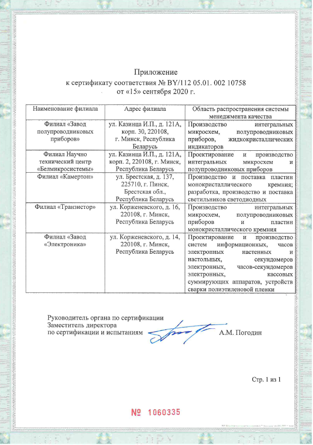
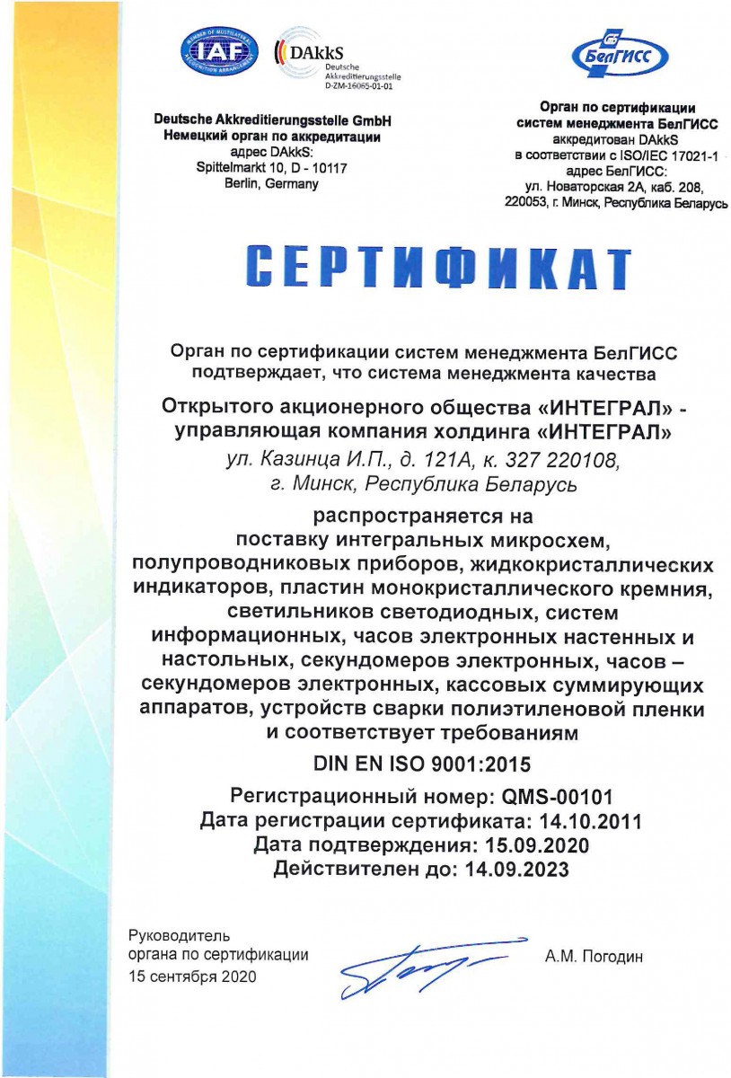
In 2021, the distribution area was expanded re-certified in 2020 by the QMS of INTEGRAL OJSC - the managing company of the INTEGRAL holding in relation to the supply of integrated circuits, semiconductor devices, liquid crystal indicators, single-crystal silicon plates, LED lamps, information systems, electronic wall and desktop clocks, electronic stopwatches, electronic stopwatch clocks, cash registers, devices for welding polyethylene film and confirmed its compliance with the requirements of the STB ISO 9001-2015 standard in the National Compliance System of the Republic of Belarus and DIN EN ISO 9001:2015 in the German DAkkS accreditation system.
In 2021 QMS JSC "INTEGRAL" is the managing company of the holding
"INTEGRAL", including the branches "Plant of Semiconductor Devices", "Transistor", Scientific and Technical Center "Belmicrosystems", "Kamerton", is re-certified for compliance with the requirements & nbsp; GOST R ISO 9001-2015 in the Electronsert voluntary certification system and applies to the development and production of electronic component base (integrated circuits and semiconductor devices) for special purposes.
In 2018, OJSC INTEGRAL is the holding's management company
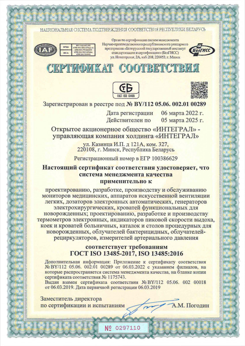
"INTEGRAL", including the branches of the Scientific and Technical Center "Belmicrosystems", "Plant "Electronics" and "Kamerton", created and implemented a quality management system in relation to the design, development, production and maintenance of medical devices, which in 2019 was certified for compliance
GOST ISO 13485-2017 in the National system of conformity assessment of the Republic of Belarus.
The functions of organizing work to ensure the effective functioning of the quality management systems operating in INTEGRAL OJSC - the management company of the INTEGRAL holding, maintaining in working (actual) condition and planning work to improve them are assigned to the quality management service, which also performs the functions technical regulation and standardization, metrological support and quality control of development and manufacturing products at all stages of their life cycle. The service reports directly to the CEO.
For the successful implementation of the tasks assigned to the quality management service, its organizational structure has a compact form and includes five internal structural divisions: the coordinating center, quality management, metrology department, standardization department and the central factory laboratory, reporting directly to the head of the quality management service, who is the representative quality guidelines.
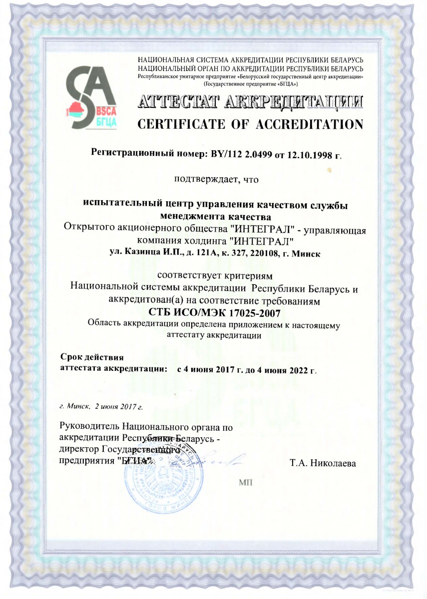
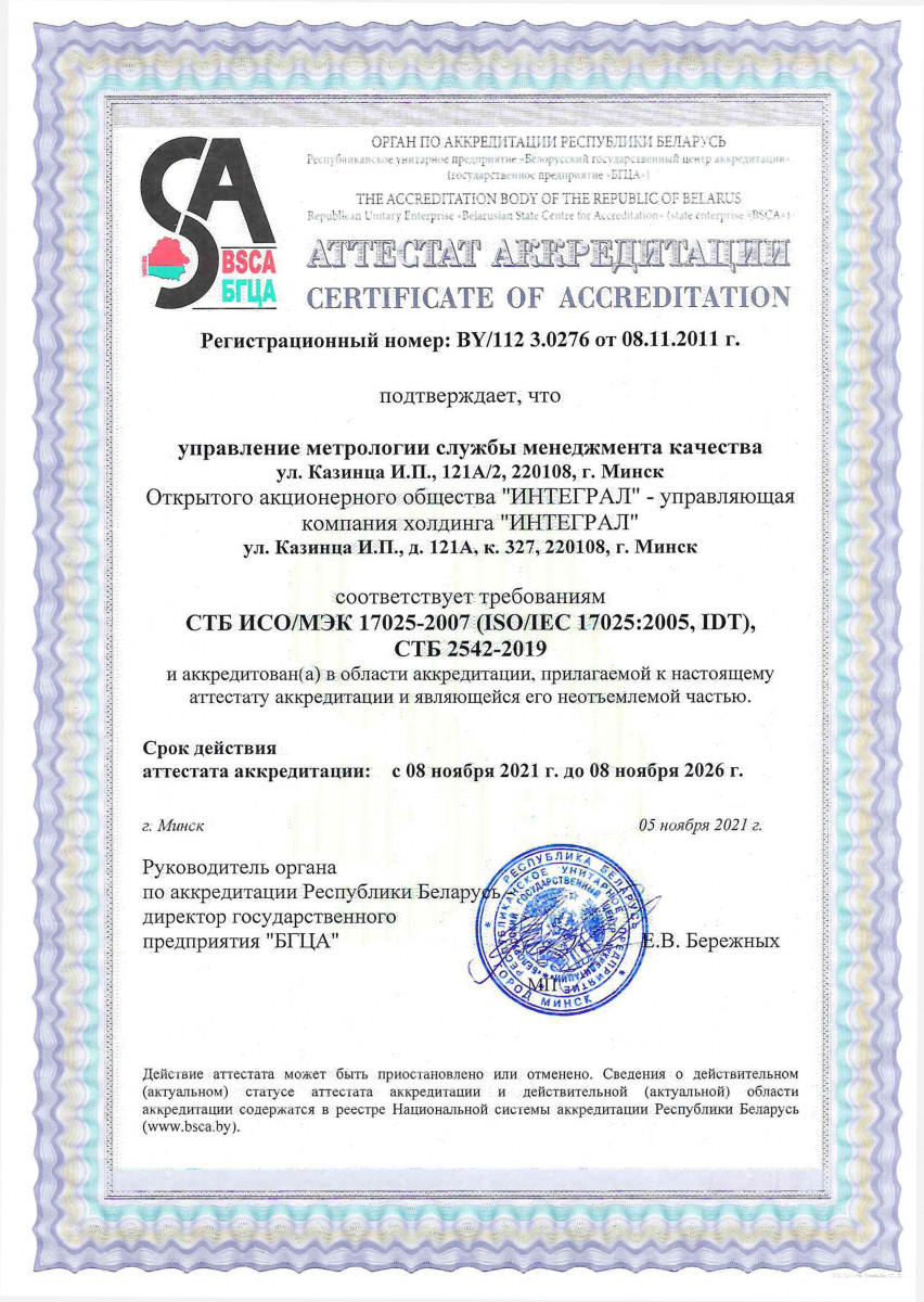
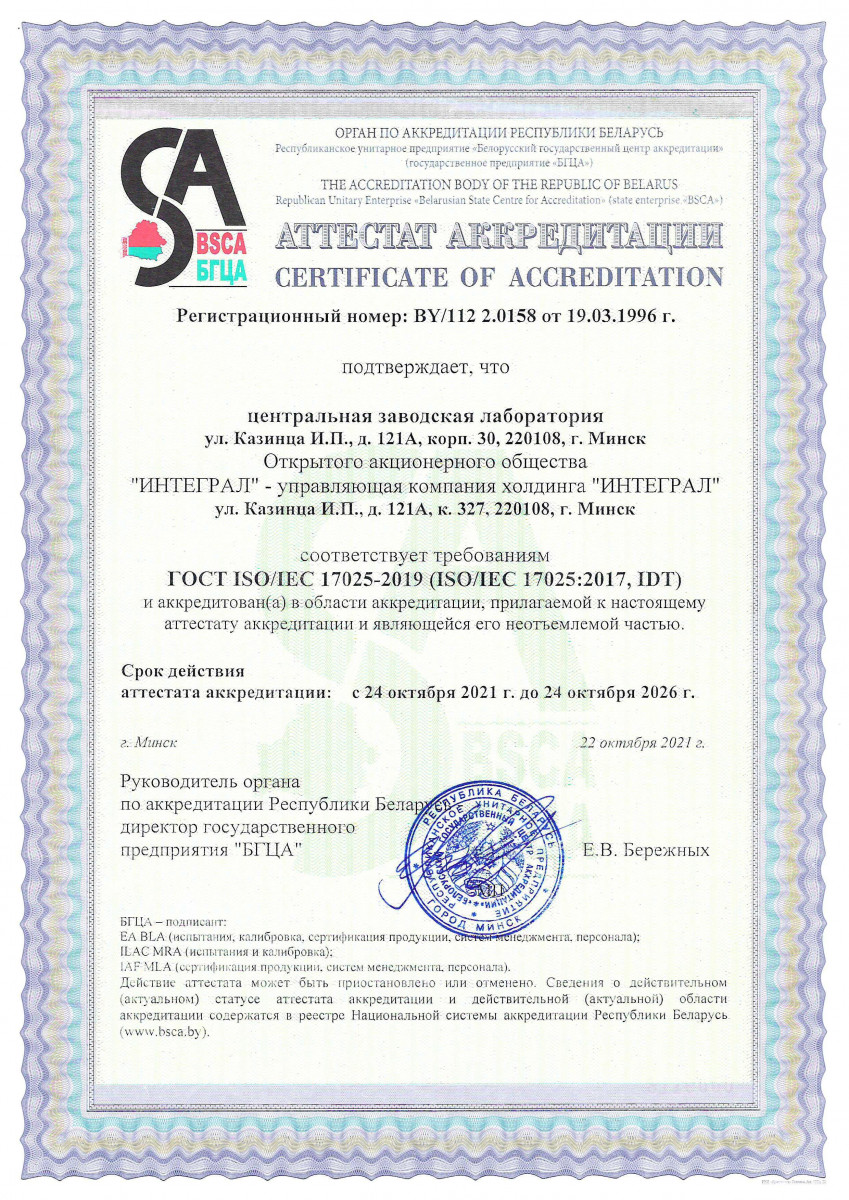
Quality Management Service of JSC "INTEGRAL" - manager the INTEGRAL holding company has subdivisions accredited for compliance with the requirements of GOST ISO / IEC 17025-2019 - a testing center for quality management, a metrology department, a central factory laboratory with areas of accreditation defined by annexes to accreditation certificates.
Quality policy of OJSC "INTEGRAL" - the management company of the holding "INTEGRAL" for 2022
Quality objectives of OJSC "INTEGRAL" - the management company of the holding "INTEGRAL" for 2022
Politics in the field of QMS quality of medical devices
Objectives in the field of QMS quality of medical devices for 2022
Information security policy of OJSC "INTEGRAL" - the management company of the holding "INTEGRAL" for 2021